AlN & AlScN Deposition Services
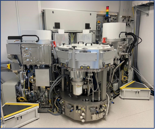
Access to advanced deposition facilities featuring the CLUSTERLINE® 200 system with comprehensive characterization capabilities.
• Co-Sputtering Chamber: In-Situ deposition of Ti, Pt, Al, Cr, AlN, and AlScN with composition control
• Single Target Chamber: High-throughput, high-uniformity AlN and AlScN deposition
• Sample Compatibility: Can accommodate samples from small chips up to 8" wafers
• Film Characterization: XRD for texture and crystallinity analysis, stress measurements, SEM/AFM for cross-sectional and surface analysis, thickness measurements, and particle counting
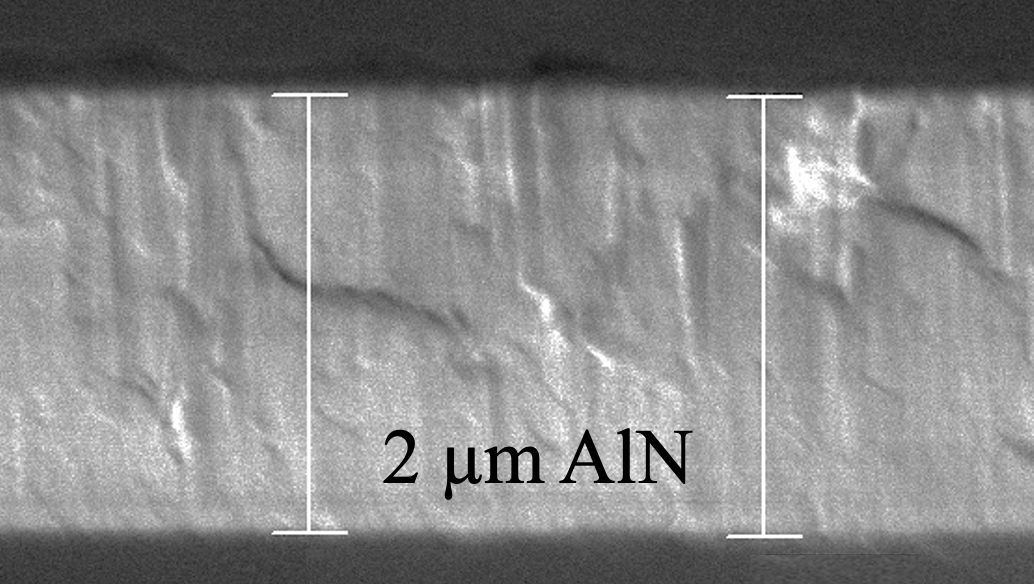
Cross-Sectional SEM
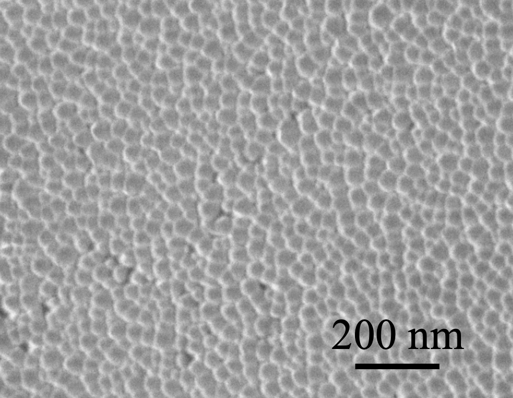
Top-View SEM
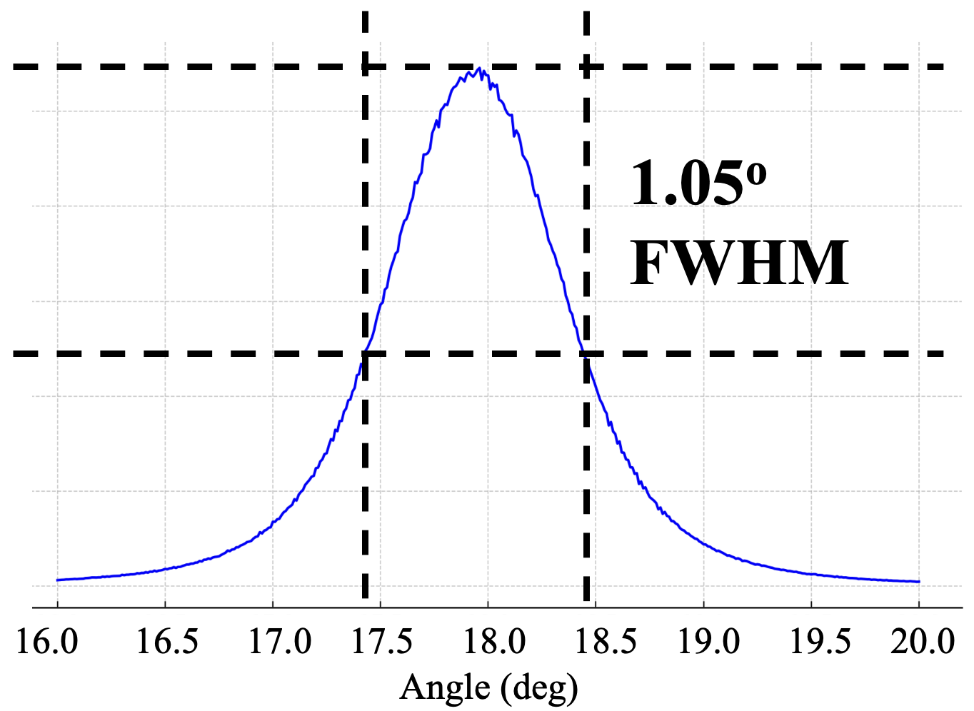
AlN Omega-Scan
Cross-Sectional SEM
Top-View SEM
AlN Omega-Scan
R&D and Prototyping Microfabrication Services
Lithography
| Tools | Type | Resolution/Alignment | Sample Size |
|---|---|---|---|
| Heidelberg DWL 66+ Low-Res Writehead | Laser Writer | 1.5 μm / ±0.5 μm | Chip - 8" Wafers |
| Heidelberg DWL 66+ High-Res Writehead | Laser Writer | 400 nm / ±0.5 μm | Chip |
| Heidelberg DWL 66+ 5" Masks Writer | Laser Writer | 2 μm / ±0.5 μm | Silica/Cr 5" Mask |
| EVG 610 | Mask Aligner | 2 μm / ±1 μm | Chip - 4" Wafers |
| Quintel 4000 | Mask Aligner | 3 μm / ±2 μm | Chip - 4" Wafers |
Deposition
| Tools | Type | Targets/Gases | Sample Size |
|---|---|---|---|
| CLUSTERLINE® 200 Co-Sputtering Chamber | Sputtering/Reactive sputtering | Ti, Pt, Al, Sc, Mo | Chip - 8" Wafer |
| CLUSTERLINE® 200 Single Target Chamber | Sputtering/Reactive sputtering | Al, Sc20, Sc30, Sc40 | Chip - 8" Wafer |
| AJA ATC Sputtering System | Sputtering | Ti, Al, Pt, FeGa, Si, SiO2, B | Chip - 8" Wafer |
| Plasma-Therm HDP-CVD | CVD | SiH4, PH3, B2H6, Ar, GeH4, O2, He, CH4, H2, N2 | Chip - 8" Wafer |
Etching
| Tools | Type | Gases | Sample Size |
|---|---|---|---|
| ULVAC NLD-570 | Deep Oxide Etcher | Ar, C4F8, CHF3, Cl2, NF3, O2 | Chip - 6" Wafers |
| Plasma-Therm ALE | ALE | BCl3, CF4, CH4, CHF3, Cl2, H2, HBr, N2, O2, SF6 | Chip - 8" Wafers |
| Oxford PlasmaLab100 | ICP RIE | Ar, BCl3, Cl2, O2 | Chip - 6" Wafers |
| Plasma-Therm 790 | RIE | Ar, CHF3, O2, SF6 | Chip - 6" Wafers |
| Pie Scientific Tergeo Pro | Plasma Asher | Ar, CHF3, O2, Water Vapor | Chip - 6" Wafers |
Metrology & Characterization
| Tool | Type | Sample Size |
|---|---|---|
| Supra 25 SEM | Electron Microscopy | Chip - 4" Wafers |
| KLA - TENCOR FLX | Residual Stress | Chip - 8" Wafers |
| Woollam ESM- 300 | Ellipsometer | Chip - 8" Wafers |
| PANalytical/Philips X'Pert Pro | XRD | Chip - 4" Wafers |
| Aixacct AixDBLI | Piezoelectric Characterization (d33, d31) | Chip - 8" Wafers |
Consulting Services
Foundry Transition
Partner with us to seamlessly transition your devices from R&D to volume production. We will help you with:
- Foundry selection
- Process design & compatibility review
- Ongoing production support
Design and Analysis Automation
Streamline your MEMS development with our advanced automation tools and custom design solutions:
- Custom piezoelectric MEMS design and optimization
- Generative layout and DRC tools
- FEM integration & automation